Logic Diagram Half Adder
Get Logic Diagram Half Adder Pictures. An logic binary adder circuit can add two or more binary bits and gives result as sum, carry. In many computers and other types of processors, adders this article gives detailed information about what is the purpose of a half adder and full adder in tabular forms and even in circuit diagrams too.
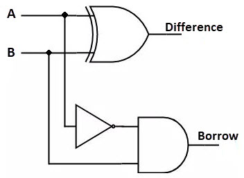
The circuit diagram for simulating the half adder above, the d.
Although by itself, a half adder is not extremely useful, it can be used as a building block for larger adding figure.1: An adder is a digital logic circuit in electronics that is extensively used for the addition of numbers. The circuit diagram for simulating the half adder above, the d. A, b and cin, which add three input binary digits and generate two binary outputs i.e.

0 Response to "Logic Diagram Half Adder"
Post a Comment