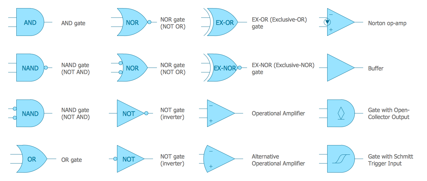
18+ Logic Diagram Not Gate Images. As by the truth table, the output of not gate will be high when the input is low. These gates have limitations for working voltage and input logic frequency.
Wiring Diagram with ConceptDraw PRO from www.conceptdraw.com Controlling a calculator display with logic gates. The switching circuit diagram of the not gate is shown below Assuming we are talking about cmos implementing not gates using nands or nors.
0v and 5v representing logic 0 and logic 1 respectively.
The diagram shows this for a. This is called logic design. In general, yes, a logic gate will have a separate power supply from its logic input. Then, we can directly convert the expression into a diagram of logic gates.

0 Response to "Logic Diagram Not Gate"
Post a Comment