Download Logic Diagram Full Adder Gif. A, b and cin, which add three input binary digits and generate two binary outputs i.e. An adder is a device that can add two binary digits.
Verilog code for Full Adder using Behavioral Modeling from www.technobyte.org Compare the equations for half adder and full adder. Full adder is used to add three bits and produce a sum and a carry outputs. Apologies, i said in the video this was a circuit diagram, i meant logic diagram.
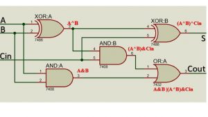
Full adder is the adder which adds three inputs and produces two outputs.
An adder is a digital logic circuit in electronics that performs the operation of additions of two number. In the block diagram, a0 and b0 represent the lsb of the four bit words a and b. An adder is a device that can add two binary digits. Compare the equations for half adder and full adder.

0 Response to "Logic Diagram Full Adder"
Post a Comment